NJQRP DDS Daughtercard Kit
Direct Digital Synthesis on a 1" x 2" pluggable card
![]()
NJQRP DDS Daughtercard Kit
Direct
Digital Synthesis on a 1" x 2" pluggable card
![]()
NOTE:
This DDS Daughtercard design is no
longer produced,
but we have a New-and-Improved
version available
for sale called the DDS-60
... 0-60 MHz coverage with
built-in DDS Amplifier and variable output level from
0 to 4V p-p, manually adjusted with a trimpot
or software controlled with a digipot.
Click
here for the DDS-60.
![]()
DDS Daughtercard (This is the original 30 MHz design, no longer produced):
This is a simple, small AD9850-based DDS board that plugs it into your favorite project to serve as a precise and stable signal source from the sub-Hertz basement all the way up to 30 MHz.
| Schematic v1.5 | Price | Resource for Soldering DDS Surface Mount Chip |
| Latest Manual v1.5 | Ordering | "VFO Control Panel" program for Win 95/98 |
| Kit Builders' Notes | Availability | Ways you can use the DDS Daughtercard |
| Kit Packaging | Obtaining a free AD9850 DDS chip | |
|
~
DDS Primer ~ |
AD9850 Data Sheet |
Original DDSVFO Article
by Curtis Pruess WB2V, QEX 1997 |
The DDS Daughtercard is once again available from the AmQRP Club, time sporting features that make it super useful in the shack and in your homebrew projects!
This run of the kit has the "good and solid" version of the MMIC amplifier we used before: the MAV-11 from Mini-Circuits. This device can produce up to 4 volts peak-to-peak signal output into a 50-ohm load, or about +7 dBm, thus enabling the daughtercard to easily drive mixers, counters and other circuits. (Changing the value of R1 can easily lower the output signal for more sensitive applications.)
This latest design regulates the supply voltage to the MAV-11 amplifier to enable the output circuit to produce a constant level signal that is always properly biased at the 60 ma design spec. In this way, the DDS Daughtercard may be used even in battery-operated projects without the concern of having the output signal level change with lowering battery terminal voltage to the board. This allows the board to generate the most optimal signal purity under all supply voltage conditions!
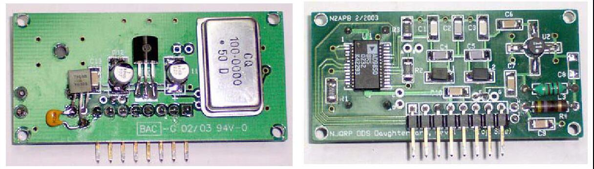
The DDS Daughtercard is shown assembled assembled. Photo on right shows top side with DDS, surface mount components for the LPF and the new MAV-11 output amplifier. [Note the new orientation of the dot on this different package.] Photo on left shows bottom side with the 100 MHz oscillator module, a 5V regulator and filter components. New components on left (L7808 regulator and radial lead capacitor) are easily tack soldered onto the same pcb as used before. Note the production-quality soldermask and silkscreening of part outlines and legends.
As
any homebrewer worth his/her salt can tell you, the Direct Digital Synthesis
(DDS) chip captures the imagination and excitement like no other technology
these days. Signal precision, accuracy, stability, programmability and RF output
quality are all easily and inexpensively within ones grasp.
But two quite formidable problems still remain.
The
first is that these surface mount chips are so tiny, with lead pitches as fine a
0.65mm, that its nearly impossible to homebrew with them using conventional
techniques. Have you ever tried tack soldering a fine wire onto one of these
small SOIC package leads?
Even soldering the chip onto a blank pc board that fans out the leads is
going to take some precision soldering and a magnifying lens on your workshop
lamp, and you end up with two layers of boards with this approach.
The
second problem is that these DDS chips must be interfaced to a microcontroller
of some sort for that frequency programmability. There are many projects around
that control a DDS chip with a PIC, an Atmel controller, a BASIC Stamp, an SX
chip, etc. I dont know about you, but the VFO I will ultimately need is
likely to use a controller that I dont technically know and cannot
program. This
makes it tough to use the controller for anything but the DDS, thus raising the
cost of the entire project, increasing the amount of board real estate needed
and raising the power needs for the entire project.
Solution
Weve created a small pc board containing just the bare DDS essentials
an Analog Devices AD9850 DDS chip, a 100MHz clock oscillator, a 5th
order elliptic filter, and a MMIC RF amplifier to boost the raw 200 mV p-p DDS
signal to a more usable 4-volt level.
The three control lines, power supply inputs, and the output signal are
available on a pinheader at the board edge.
The simple schematic is shown below.
The
8-position pinheader at the board edge serves to allow DDS Daughtercard to be
plugged into whatever project you might have on your bench, regardless of which
microcontroller is being used.
Thus you are not locked into using an Atmel device if your preferred
controller is a PIC. Just
provide a single strip socket (e.g., a 16-pin IC socket split lengthwise) on the
project board and plug in the DDS pc board. Heck, you dont even need a
microcontroller with this approach just wire the pinheader signals over to a
cable on the parallel printer port of your PC and use public domain PC software
to control the DDS board!
The
controllers software just needs to send a 40-bit serial data stream on the
DATA line with each bit being clocked by the CLK control line.
At the end of the sequence, the LOAD line is toggled to instruct the DDS
chip to use the new frequency then bingo, the new frequency appears
on the output of the DDS board at pin 8.
The
programming sequence can be easily accomplished.
Joe Everhart, N2CX uses the following three lines to instruct a BASIC
Stamp to produce a 7.040 MHz signal with the DDS Daughtercard on the QuickieLab
shiftout 7,8,0,[$02,$BC,$05,$12,$00] shift out 40-bit value on port P7 using P8 as clock
out9 = 1
toggle the line
out9 = 0
going to the DDS load pin
This simple DDS daughtercard project solves both of the problems cited at the top of this page, and enables homebrewers to easily take advantage of the positive attributes of the DDS chip to produce high-quality homebrew variable-frequency signals.
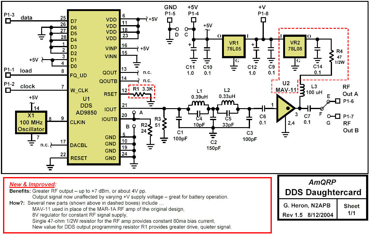
Schematic for the DDS Daughtercard, rev
1.3
(View or download a hi-res PDF version)
An interesting option -- "Dual VFO"
The
Daughtercard's pc board was designed to present an interesting option for the
homebrewer. The AD9850 DDS chip offers a complementary output at IoutB (U1 pin
20), which is sometimes uses to feed the low pass filter along with the primary
output signal IoutA to produce an output signal of even greater spectral purity.
(Refer to the AD9850 data sheets for these details.)
However, this secondary signal is not quite 180-degrees out of phase from the
primary but one may experiment and
possibly find useful applications for it using this capability. If this IoutB
signal is to be used, a low pass filter must also be used to clean up its output
and thats where the DDS Daughtercards design options come into play.
So, what can you do with a "DDS daughtercard"?
There are many ways for you to use the DDS Daughtercard. Essentially, all you need to do is combine it with your favorite microcontroller project to form a high-quality VFO. Click here to see lots of ideas!
Getting a FREE DDS chip from Analog Devices
The AD9850BRS DDS chip is not provided in the DDS Daughtercard Kit because homebrewers can obtain a free sample from the Analog Devices website at http://www.analog.com/en/prod/0,,770_843_AD9850,00.html#price. Just go to this Internet location, register with Analog Devices (i.e., give them your mailing address), and within a week or so you will receive a free sample of the DDS chip by mail.
Need help attaching the DDS surface mount chip?
If
desired, the NJQRP has lined up a great resource to assist in soldering the DDS
chip onto the printed circuit board. Once youve acquired your free AD9850BRS
DDS chip from Analog Device, send the chip and your DDS Daughtercard circuit
board, to Mike WA6OUW, at KitBuilders. For $6 he will attach
this surface mount chip to the pc board and return it promptly by mail. Its
not tested because at that point its only the DDS chip on a bare pc board,
but Mike does excellent work. (The NJQRP uses KitBuilders for assembly of the
HC908 Daughtercard product, so we know the quality is there!) Just place your
DDS chip, pc board and a $6 check or M.O. payable to KitBuilders into a
padded envelope and send to: KitBuilders,
You won't believe the packaging of this kit. When you stop to think about it, it can get rather tricky kitting up a project that uses those tiny surface mount chips. Tom and Nancy Feeny (W8KOX and NJ8B) tackled this problem for us and came up with a brilliant way of doing it. We won't give away all their secrets, but they ultimately provided all SMT chips taped onto a color-coded strip of paper. You've *just* got to see this one to believe it. Their technique makes assembly of the kit foolproof and simple. Just slice the tape next to the component you are next installing, remove the part with tweezers and solder it onto the board!
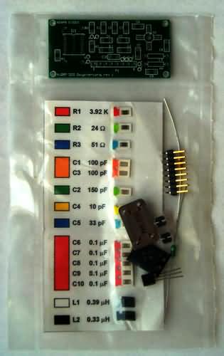
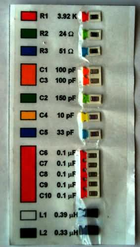
W8KOX and NJ8B made up the DDS Daughtercard Kits for us using a splendid color-coded technique that makes parts identification a breeze
Availability
This
DDS Daughtercard design is no longer produced, but we have a New-and-Improved
version available for sale called the DDS-60
... 0-60 MHz coverage with built-in DDS Amplifier and variable output level
from 0 to 4V p-p, manually adjusted with a trimpot or software controlled
with a digipot.
Click
here for the DDS-60.
![]()
![]()
%20-1.JPG)
%20-2.JPG)
%20-3.JPG)