 Digital
QRP BreadBoard
Digital
QRP BreadBoard |
Digital
QRP BreadBoard |
|
Digital (column #4)
Schematic
for
Antenna
Analyzer photo
Source
Code for
Binary
Hex Code for
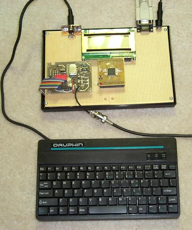
BreadBoard
photo
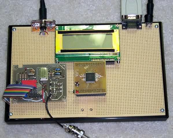
BreadBoard
photo
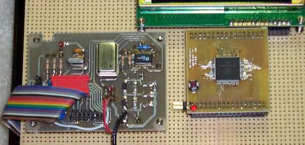
BreadBoard
photo
BreadBoard
Schematic
BreadBoard
Schematic
Back
to
|
SWR
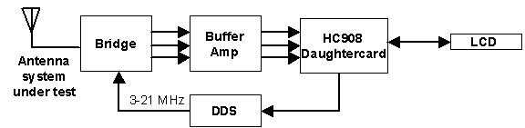
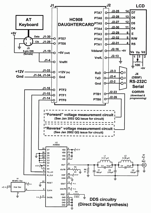
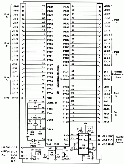
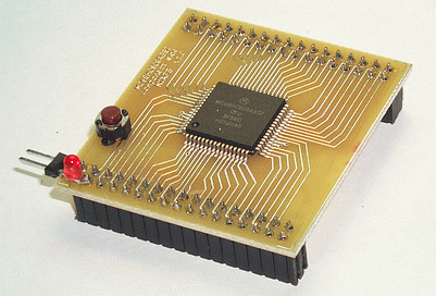
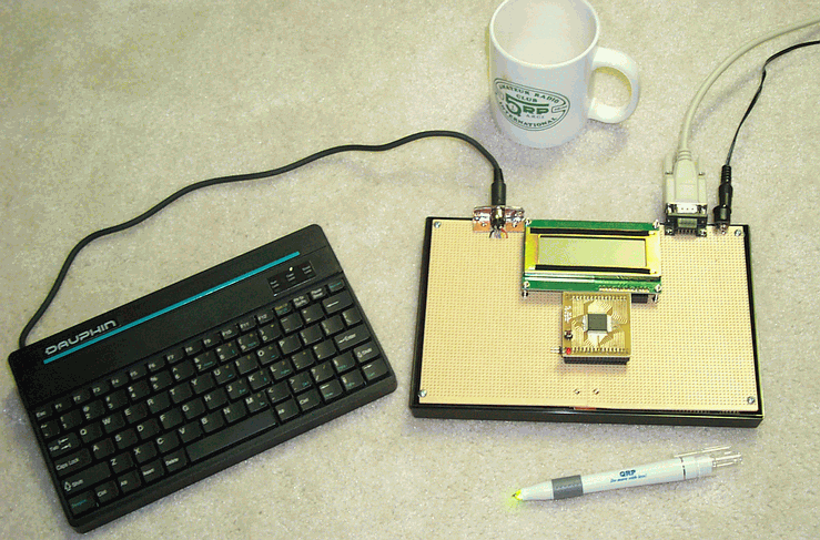
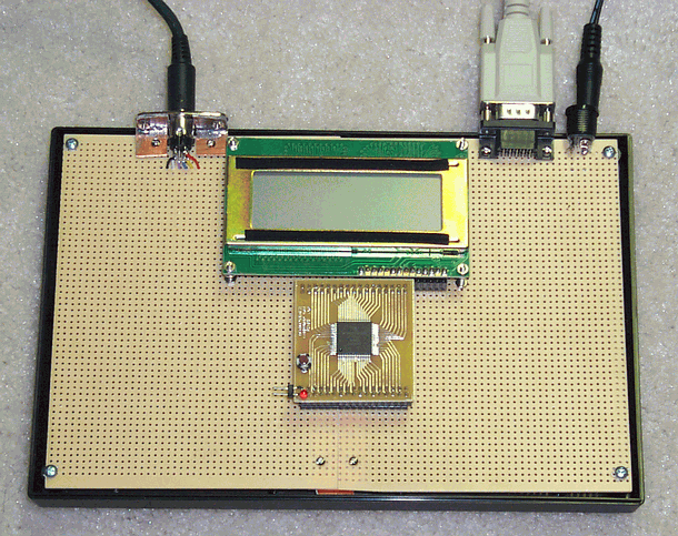
Measurement Software and Hardware This is the fourth installment of our evolving Digital QRP Breadboard project and were ready for the first real application. Last time, I mentioned an exciting milestone looming ahead for this project ... and were now prepared to state that milestone is an antenna analyzer. This installment will establish the algorithmic and computational foundation necessary for us to get there. As a short recap, lets first overview where the project currently stands. Review of Current Status So far weve developed a small computing module called the HC908 Daughtercard that is the brains of the project. It holds the Motorola 68HC908AB32 microcontroller unit (MCU). This self-contained 8-bit microcontroller runs at 8 MHz and has a memory complement of 32 KB of programmable FLASH for program storage, 1K of non-volatile EEPROM for calibration and data constants, and 1KB of volatile RAM for variable and temporal data storage. The HC908 has 51 programmable I/O bits, with some dedicated and built-in higher level blocks for A/D conversion, timing and serial port registers. The microcontroller is mounted on a 2 square pc board that plugs into the main board of the Digital Breadboard, or into any other project you might have on your workbench. Other components on the Digital Breadboard include a 4 line x 20 character LCD, an input port for a common IBM PC compatible keyboard, and a Direct Digital Synthesis frequency source. [To see an example of how the HC908 Daughtercard can be used in other custom projects, see the web page wherein I describe the "HC908 Commander - An Intelligent Controller for Ham Radio Control". This application of the HC908 Daughtercard was presented in my Micro Moments section of QRP Quarterly's Idea Exchange column for July 2002.] Of course, there is software glue that holds all these components together, enabling it to actually do something for us. Thus far, weve developed simple programs to input characters and voltages that get displayed. We can also generate any given frequency from the sub-Hertz region up to 20 MHz. These are useful building blocks or routine libraries, but as yet they perform no synergystic purpose. This condition will change with the project updates this time. Antenna Analyzer Building Blocks Now that we have some project basics in place -- computing module, I/O devices and a user interface -- well start developing some functional building blocks that we later use to make a full piece of test gear for the bench. Were going to start by building a basic absorptive SWR bridge that will be driven by the computer-controlled frequency source presented last time (i.e., the DDS) and whose output will in turn drive an antenna system. The analog results of the SWR bridge will be read by the built-in A/D converter on the HC908 microcontroller. By sweeping the DDS frequency across a given ham band and computing the SWR of the antenna system at various points along the way well have ourselves a rudimentary antenna analyzer. Refer to the block diagram in Figure 1 that illustrates this system.
Figure
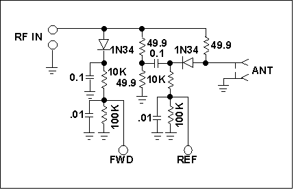
1: Block diagram of the SWR measurement system SWR Bridge & Diode Detector Referring to Figure 2, a Wheatstone bridge is composed of 50 ohm resistors with the antenna as the unknown leg of bridge. When the antenna is at resonance, presenting a minimum impedance with a pure 50-ohm resistive real component, the bridge is balanced and the AC voltages on each side side of the bridge are identical. No AC current flows between the legs.
Figure
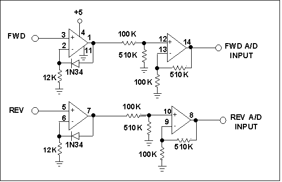
2: Schematic of the SWR bridge and diode detectors However when the antenna system is not resonant, the complex impedance of the antenna is not 50-ohms but something greater, which creates a bridge imbalance. The 1N34 diode samples that AC signal imbalance, rectifies it, and after filtering, the DC signal is directly analogous to reflected sample of more familiar SWR bridges. We then sample the forward power using another diode detector on the original incoming signal. These forward and reflected DC signals are presented to the next stage for compensation, buffering and amplification. Buffer Amp There are two reasons for employing the op amp circuits in Figure 3. The first amplifier in each path (FWD and REV) compensates for the nonlinearities in the diode detectors when the bridge is operated at very low power levels. These first stage op amps employ 1N34 diodes in their feedback paths to counteract these nonlinearities in the bridge diodes. This action essentially moves the natural knee of the curves closer to zero, thus improving the accuracy of the readings FWD and REF readings ultimately presented to the A/D input on the microcontroller.
Figure 3: Schematic of the LMC6485 buffer amp The second purpose for the op amps is to amplify. The DC signal levels coming from the bridge, and through the unity gain of the first compensation stage, are fairly low. In order to make the most use of the 8-bit A/D, we need to amplify the detector voltage up to the 5V range of the A/D. Further, the output of the op amp circuits is quite low which provides a better condition when presenting signals to the 10K input impedance of the A/D. (The output impedance of the diode detectors themselves is approximately 100K-ohm. If those signals were directly input to the A/D, they would be greatly affected by the lower impedance of the A/D.) Building the Bridge and Amp Recalling that weve already constructed the other major system components in previous issues - the HC908 Daughtercard microcontroller, LCD, and DDS - all we need to do is build up the breadboard/prototype SWR bridge and compensation amplifier. Of course later down stream well have a pc board developed for all of this, but for now youll be able to participate in the evolution of the project by homebrewing the project along with us here. No special cautions are necessary concerning the construction of either board. In the examples shown in Figure 4, Manhattan style construction was used to make the bridge board, and perf board construction was used to create the amplifier board.
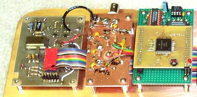
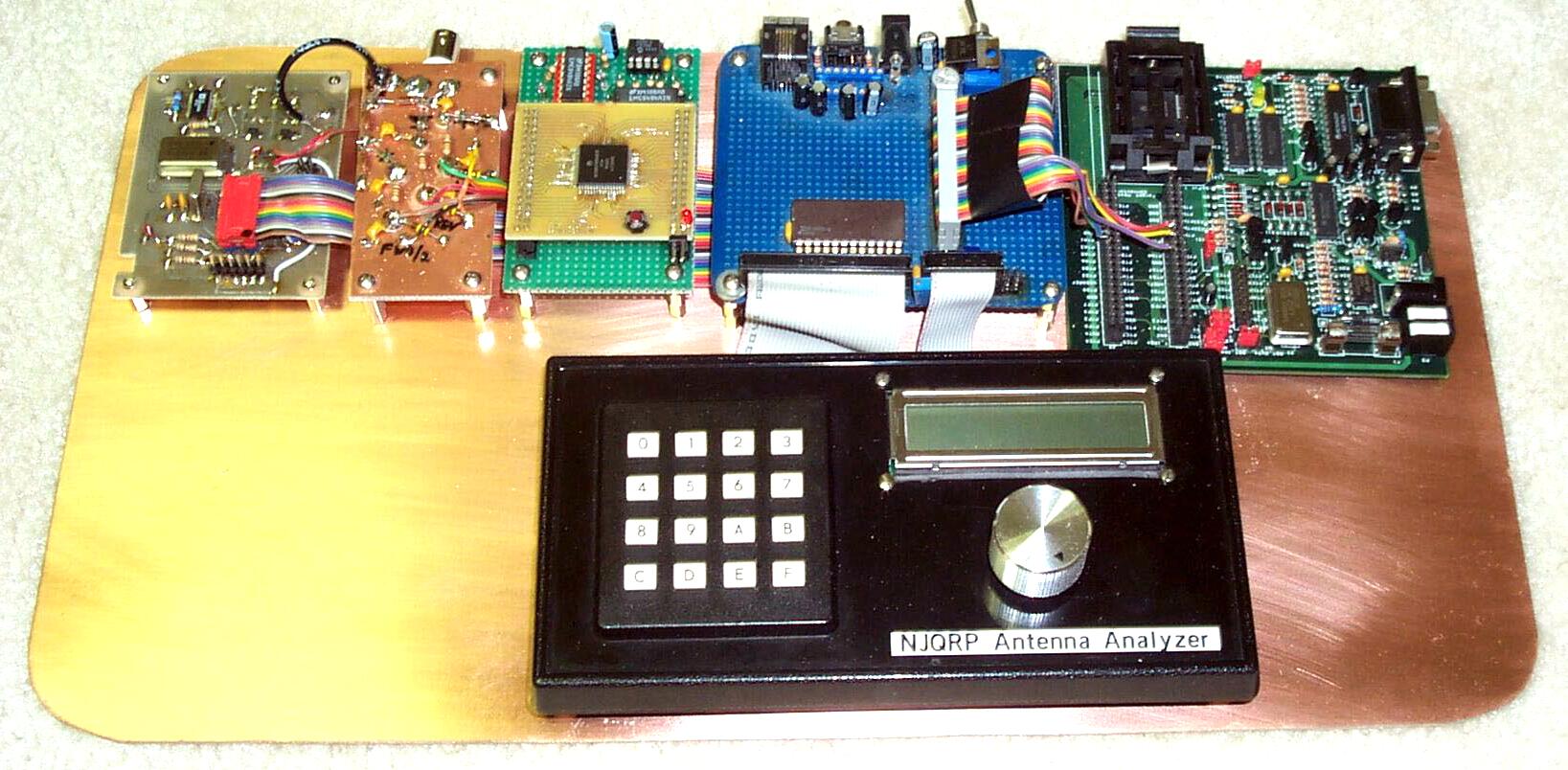
(Click here or on photo for higher-resolution image) Figure
4: Photo showing layout of the project during
heavy-duty debug. Shown L-R
are the DDS board, the SWR Bridge, and the Buffer Amp with the HC908
Daughtercard plug-mounted above it. A base board supplying the power
and connecting the LCD are off the photo and not shown. Connecting the Modules Referring to the overall schematic for the simple antenna analyzer in Figure 5 youll see the how the whole system is connected together. I think youll agree that this shows just how simple and straightforward the hardware design can be for an antenna analyzer. The HC908 Daughtercard is at the center of the project - literally in concept and physically in the schematic. The functionality packed into that 2 square board allows us to design a significantly capable instrument by only adding a few other components. Software Makes it all work! As usual, the software program were describing here is downloadable from this site. You can download the binary hex code as is to yield a basic antenna analyzer instrument as described here. Alternatively, you can using the source code as a starting point for making your own specific enhancements and custom modifications. Let's walk through the algorithm a bit, as seen in the "mainline" routine at the start of the program. After power is applied and the initialization of I/O devices and variables is done, the mainline of the program is executed. The mainline is a simple loop that performs the following actions over a pre-determined range of frequencies:
When the scan is complete, the program analyzes the list of scan data to determine antenna resonance (the frequency of the minimum data point) and the Q of the antenna system (how sharp the dip is). Setting the DDS Frequency The DDS frequency, phase and control bits are serially delivered to the device via three I/O lines coming from the HC908 Daughtercard: data, clock and load. Per the details provided in the AD9850 data sheet, the HC908 delivers these 40 bits of programming information by repeatedly setting the data line to the desired value, and toggling the clock line in order to move the data bit into the DDS chip. After 40 such bit clocks, the load line is toggled which instructs the DDS chip to put that 40-bit programming word into effect. At that point, the output of the DDS changes and the new frequency is present on its output. Display Frequency on LCD The frequency is displayed to the LCD by placing the binary coded decimal (BCD) value of each digit into seven sequential locations LCD_dat+0 through LCD_dat+6. These digits represent the 10 MHz position through the 10 KHz position in the frequency display. The LCD driver routines take these BCD numbers and dipslay them to specific locations in the LCD memory, thus making them appear on the display itself. The numbers contained at these locations represent the start of increment/decrement functions (used in scanning), and in subsequent calculation of the DDS programming 40-bit word (used in setting the DDS frequency.) Read Analog Signals The forward voltage FWD and reverse voltage REV are merely read as 0-5V analog voltages by the A/D converters built into port D of the HC908. These 8-bit converters quantize the analog signal to one of 256 values, based on the analog signal presented on the respective port D input pin. Thus a granularity of 19.531 mV is achieved. This level of precision is entirely adequate for determining even the low-end knee of the diode detectors primarily because of the compensation diode placed in the second op amp circuit for each signal path. Compute the SWR Using measured values to calculate SWR means that instrument is self-calibrating. This is a good thing in test equipment! The following simple equations are coded in the software, using the FWD and REV signals read by the A/D.
Store the SWR in list Each frequency samples computed SWR is stored in a list in RAM memory for processing at the conclusion of the scan.
Next Time ... Thats it for now. Enough information has been presented described here and on our companion web page to allow most homebrewers the opportunity to get a rudimentary frequency scan and SWR analysis loop together for the antenna system at the home QTH. You know where your antenna is resonant - that is, which frequencies is it tuned for - and you can check the operation of your evolving Digital Breadboard against that known condition. In the next project installment (October 2002) well add a few more human interface components and corresponding software modules to complete the antenna analyzer application of our Digital Breadboard. This work will result in a real usable piece of test equipment for the shack. Then in the following issue (Jan 2003), well introduce a small DSP plug-in card that will allow us to perform audio modulation and demodulation functions ... leading up to a standalone portable PSK31 station"! Indeed there is much more fun ahead. Please feedback on how you are enjoying the project and what uses you are planning for the Digital Breadboard and the HC908 Daughtercard. Who knows, maybe we can collaborate on a project together and chronicle its development here in these pages! Page last modified:
July 31, 2002
|