![]()
SNAP
Application Notes
![]()
by
Joe Everhart, N2CX, for the NJ-QRP
Club
Introduction
The SNAP is a simple one-transistor crystal oscillator that can be used as a low-power transmitter. It was designed by Chuck Adams, K7QO, and distributed to attendees of Atlanticon 2000 by the NJQRP Club. It is an excellent vehicle for experimentation with RF circuits and "Manhattan-style" construction. And as early builders of the project have discovered, it can even be used to make cw contacts!
This note will describe the circuitry, give some ideas for modification and even some "add-ons" to make it more useful as a transmitter. The SNAP's simplicity and construction make it an ideal learning tool that can be easily modified to try different component values and configurations.
Two excellent references that every homebrewer should have are any recent addition of the "Radio Amateur's Handbook" and "Solid State Design for the Radio Amateur." Both are available from the ARRL and provide invaluable resources for learning more about radio circuit theory and operation. Reference to them will be by the abbreviations "RAH" and "SSDRA."
The circuit descriptions and modification suggestions to be offered are based on "paper analysis" so they should be treated as such. Your mileage may vary. And don't take any of the suggestions as criticism. The SNAP is a marvel of simplicity which makes it a good learning tool and one good way of learning is by making modifications to see what works and what does not. And it is your duty while doing this to learn just what is happening.
SNAP Circuit Description
Figure 1 shows the SNAP circuit diagram. The SNAP is a one-transistor crystal oscillator that provides a milliwatt-level 80 meter CW signal. It can be used as a stable signal source at approximately 3.58 MHz or even a very simple transmitter.
The SNAP uses a Colpitts oscillator configuration modified by placing an RF transformer in the collector circuit to extract RF output. Bias to transistor Q1 comes from resistive divider R2 and R3 and emitter resistor R1. Transistor operating current is set by the drop across R1. Numerical estimates of the bias levels will be discussed later.
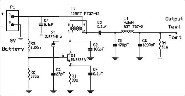
Figure 1: Schematic of the SNAP
Crystal X1 oscillates between its series and parallel resonant points where it "looks" like an inductor. Capacitors C1 and C2 comprise the capacitive divider which form the remainder of the Colpitts circuit. C4 is a bypass capacitor which ensures that Q1's emitter is at ground potential.
C3 provides DC isolation to couple RF energy from T1 (more about T1 shortly) to the output filter circuit. Inductor L1 and capacitors C5 and C6 form a Pi-type lowpass filter to give a clean sine-wave output. For testing purposes R4 is connected to provide a 51 ohm load. When the SNAP is used as a transmitter, R4 is disconnected and an antenna can be connected in its place.
Both the output pi filter and transformer T1 transform the 51 ohm (or approximately 50 ohms with an antenna) load impedance to a higher value at Q1's collector. This controls the operating power level of the oscillator so that a reasonable amount of power can be extracted while ensuring that the oscillator isn't loaded too heavily.
DC power comes from a 9 volt battery connected to plug P1. Nominal DC drain is about 20 to 30 ma so an alkaline battery will give better results than the more common carbon-zinc or so-called "heavy duty" flashlight batteries. The latter will work but battery life will be short and RF from the SNAP will drop quickly as the battery voltage drops. C7 is an RF bypass capacitor that ensures a good low impedance power source.
Detailed Analysis
Static bias current can be estimated by using some simple math. Resistors R2 and R3 establish a base voltage of about .69 volts assuming negligible loading by Q1. Now the base-emitter junction of Q1 has a drop of about 0.6 volts (it is a forward-biased silicon diode) putting .09 volts across emitter resistor R1. This establishes an operating current through the collector and emitter of 2.3 ma. However measured values of power drain are about 25 ma. How is this possible???
Well look at the first word in the paragraph above it is "static." This is based on the assumption that RF signals in the circuit are small enough that they don't affect biasing. That is often not a good assumption in oscillators!
Positive feedback is what allows them to generate a signal in the first place. But unchecked positive feedback would allow voltages and power to keep increasing forever. Now the conservation of energy principle won't allow power in a circuit to exceed what it can get from its DC source. What actually happens is that at some point either the circuit voltages and currents reach a limiting values. This can be clipping at ground on the bottom of the collector sine wave, exceeding twice the supply voltage at the collector (resonant circuit flywheel action allows the sine wave to swing above the DC supply value) or the transistor gain may drop at an extreme of the sine wave limiting available gain. Actually there *is* another limiting case where the energy gets so high that it zaps a component but that's not a very useful circuit!
The net effect of the limiting is that it can shift bias currents in the transistor well away from the static calculated values. Thus exact analysis of oscillators is best done using computer tools like SPICE or the circuit can be built and measured. (Jim Kortge, K8IQY has contributed a SPICE model for analyzing the SNAP circuit within Electronic Workbench. This model is presented in the Appendix.)
The oscillator operating frequency is set by the crystal X1, and feedback capacitors C1 and C2. The exact values of C1 and C2 also affect the excess gain available so that the circuit can oscillate. They are usually sized somewhat larger than the values used in the SNAP. For simplicity's sake the values chosen present a load capacitance near 30 pf so that it oscillates near the expected frequency of 3579 KHz. Possible variations will be discussed later. Check the RAH and SSDRA for more detail on crystals and crystal oscillators.
Because an oscillator is a nonlinear circuit estimation of its exact output power is as difficult as figuring its bias. Again, a SPICE simulation or empirical determination are in order for accuracy. However a maximum value can be estimated. The Pi output filter transforms the 51 ohm load resistance up to about 480 ohms. This is further stepped up 4 times by T1 to present an effective load impedance of about 1920 ohms at the collector of Q1. This will allow a theoretical maximum power of about 40 mw to be generated. This is an upper value and it is based on a number of assumptions so it will likely not be seen in real life.
Like any practical circuit, the SNAP has limitations. Compromises were made in its design that can be challenged to optimize one or another aspect of its performance. As you might expect, though, "souping it up" to improve it in one way will affect its other characteristics. Let's look some changes you can try.
Getting More Power From Your SNAP
Previous analysis has shown a theoretical maximum power of 40 mW. Most SNAPs produce only about half as much as this. Things that limit achievable power include transistor gain, operating bias, crystal activity, component loss, component tolerances and tuning of the output filter. You cannot expect to get too much power from a crystal oscillator. Trying to get too much power out is complicated by the fact that if you take *too* much power out you won't have enough feedback for successful oscillation. And excessive feedback may damage the crystal.
The effect of transistor gain can be checked simply by using a socket for Q1 and plugging in different devices to see if you can get more gain. You will likely not see more than a 10 or 20% variation.
Operating bias will be affected by battery voltage, component tolerance and transistor characteristics. The static value is strongly affected by the exact values of R2 and R3. Remember that the nominal value is about .69 volts and the transistor sets the .6 volt drop to emitter resistor R1. For example if the base voltage falls below .6 volts the transistor might not even turn on! And if it increases to .78 volts, the R3 voltage will double, causing the bias current to double. A more conservative bias scheme would use a larger value for R2 resulting in a higher base voltage to lessen the effect of base-emitter drop. R1 would also be increased to keep the same transistor operating current. In real life, things might not be that drastic since the oscillator tries to adjust bias by itself.
Crystal activity can be gauged by how well the oscillator tolerates keying. If it is sluggish to start when turned on and off or chirps when monitored in a receiver, you can suspect low activity which means that the crystal's loss resistance is too high. Swapping crystals to find one with lower loss can cure the sluggish oscillation and possibly increase power output slightly.
Most "crystal Colpitts" oscillators use larger feedback capacitors than the SNAP does for C1 and C2. Lower reactance and component values closer to equal for these two parts can result in more stable operation, possibly higher power out and less of a tendency for the crystal to oscillate at an in its overtone mode (approximately 3 times the marked frequency). This latter handicap has been noted by some builders since some crystals my favor their overtone due to the relatively low C1 and C2 capacitance and the low Q of the output filter network. Generally the feedback caps should be in the area of 220 to 330 pf for 80 meter oscillators+. However this will "pull" the operating frequency down closer to the crystal's series resonance. Placing the 27 of capacitor between X1 and Q1's base should raise the frequency slightly.
Some SNAP builders have been able to cure sluggish startup and overtone oscillation by grounding the crystal can. This reinforces the notion that larger feedback capacitors might be in order.
Finally, it is possible to increase SNAP power out by decreasing the impedance reflected back to the collector by changing the values of C5, C6 and L1. L1's apparent inductance can be increased slightly by squeezing its turns closer together or decreased by spreading them apart. If you want to significantly change the network's impedance transformation characteristics check out the references for Pi filter calculations.
Remember that all of the above circuit "tweaks" interact. It's like when you poke a balloon. You may dent it inward in one place, but it squooshes out somewhere else. And drastic changes in output power are likely to affect output harmonics.
Simple Keying Circuit
The SNAP is so simple that it doesn't include a means of keying. Folks who have used their SNAP on the air have simple connected a key in series between the battery and the SNAP. This works ok with a straight key but most keyers are set up to ground a rig's key line. Figure 2 shows a simple one-transistor switch that will allow using a keyline-grounding keyer with the SNAP.
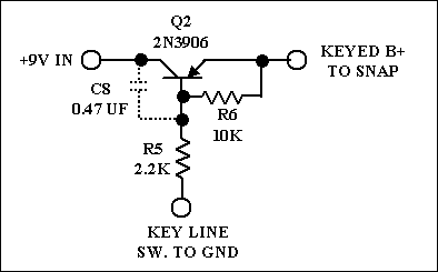
Figure 2: SNAP Switch for grounded Keyers
When the input keyline is in the "key-up" state, PNP transistor Q2 sees no base current so it feeds no power to the KEYED B+ output. Grounding the keyline draws base current through R5 turning Q2 on. It then becomes a low resistance feeding full voltage to the SNAP connected to KEYED B+. Capacitor C8 is optional and is needed only to "soften" Q2's turn on and off is keying is too sharp causing on-the-air key clicks.
Popping a FET Onto Your SNAP to Give it More Crackle
As mentioned earlier, it is tough to get significant RF output from a crystal oscillator. So adding an amplifier is a reasonable thing to try. But in keeping with the minimalist spirit of the SNAP we don't want to strap on much of an afterburner. Figure 3 is the a possible circuit for some small "boots" to boost power a little. It is a more-or-less class C FET amplifier that can produce as much as 800 mw from a 9 volt supply. You *can* get more from a 12 volt supply but 9 volts is chosen so that it can run off the same battery as the SNAP.
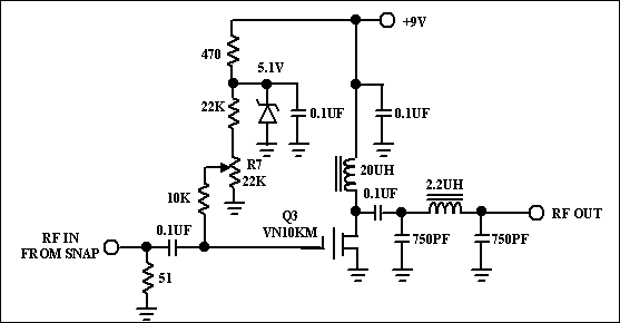
Figure 3: Simple FET amp
for SNAP gives up to 800mW out
RF from the SNAP is about 3 volts peak-to-peak assuming approximately 20 mW is produced across a 50 ohm load. VN10KM transistor Q1 is an N-channel enhancement-mode FET which has a turn-on voltage of between 1 and 2 volts. So the 3-volt RF from the SNAP is just about right to operate it in Class-C. A slight positive bias voltage is applied by potentiometer R7 to allow adjustment bias adjustment for best operation. It should be adjusted for no bias current through Q3 with no RF input. Fine adjustment can then be made with RF drive allied to set power output. Q3's DC power is supplied through L2 and a simple PI filter gives harmonic suppression. This is an experimental circuit so its performance is not guaranteed.
Parting thoughts
These notes are intended to give some ideas about how to customize your SNAP. They are not complete and for best results a fair amount of reading outside reference material, experimentation and maybe even some good analysis with a computer tool such as SPICE will help you get the most out of your SNAP. Most importantly build it, play around with it and report your successes and failures to the QRP community so that we can all learn. Enjoy!
Joe Everhart, N2CX
214 New Jersey Road
Brooklawn, NJ 08030
email: n2cx@voicenet.com
Return to the Atlanticon home page
![]()
![]()
![]()